I was not successful with AN758. It is behind me now. Our group is now building 25 of the HF SuperPacker Pro 100W Amp V2 projects.
http://site.hfprojectsyahoo.com/hf_superpacker_pro_ver_2
73, K5OOR – Virgil

I was not successful with AN758. It is behind me now. Our group is now building 25 of the HF SuperPacker Pro 100W Amp V2 projects.
http://site.hfprojectsyahoo.com/hf_superpacker_pro_ver_2
73, K5OOR – Virgil
The development wheel continues to turn slowly. I finally received the LM723C replacement part. Through a blog post from a member, I was alerted that the series pass transistor, Q3, substitute provided by CCI has a reverse pin out from the circuit board. I replaced that part as well as I installed the replacement LM723C. A check on the bias now under RF load shows that it stays stable at about 0.7V bias. The RF output doubles with a doubling of the RF drive input (1W to 2W).
That being said, the RF output is still very low (only about 10W max). I can crank up the drive to draw about 4.5A from the transistors. I don’t know where the RF is going but it is not reaching the output. I reviewed the T1 connections and looked for balanced gate signals with the scope. I reviewed T2 to make sure that was correct. My next thought is to remake T3 with short leads but I think that will not be the answer. I am going to test the T3 circuit independently to make sure it is working and delivering RF power to the load before re-installing.
I ordered a used HP Model 428B clip-on current meter so that I can see the DC current for each transistor.
I really thought I was going to be up and running with the AN758 Amp without any problem before now. That just proves that you can’t get sure of yourself as if all this was easy. I appreciate your feedback and experience with the AN758 amp assembly and test.
The AN762 Amp was not a problem in the past although I did make about 5 prototype layouts before I was happy with it.
73, K5OOR – Virgil
I have the amp together and attempting to run it.

The kit did not provide any hold down washers or any mention about how to mount. In the AN758 document picture it looks like fiberglass oversize washers. No matter, it is just for testing as a bench mark. The assembly took longer than expected because the documents were wrong and incomplete. See the markup corrections I made. Rather than loose this information, I wanted it to be available for other builders.
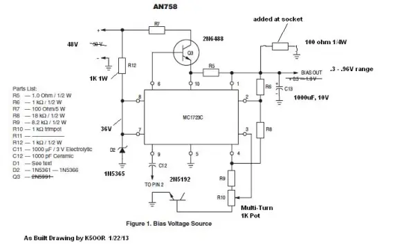
I changed the 1–turn pot to a 12–turn pot (same foot print). The zener supplied was a 45V device which is over-voltage for the MC1723C part. I changed to a 1N5365 36V zener. I added a 100 ohm pull down resistor on the bias supply so that the bias voltage would not float when the 48V was not present. I recorded the voltage range I obtained with adjustment. I added a 0.01uF cap across C13 for high frequency suppression. More about operational testing after showing you the amp schematic as built.

This schematic had a comedy of errors everywhere you look. I think I have it straightened out with the values I used to build this bench mark amp.
TESTING – I was able to easily set the bias. I used the recommended 300mA as a starting point. I have a 4dB resistive pi network on the input of T1 just to make sure the amp was seeing 50 ohms drive impedance. I keyed with 2W, 3W and 4W. My test was on 80M. I only measured about 10W with 2W drive. I expected it to double with 4W drive. The output only increased about 2W! So, I started trouble shooting and found that the bias supply is not stiff. It sags big time and has RF on the output. I know from past experience that the bias supply is very critical to the amplifier performance and it must be very stiff and transient responsive. This particular part obviously is not.
The only explanation I have, at this point, is that I caused a failure of the part when the wrong specified zener was in circuit and the Vc (pin 7) exceeded the 40V maximum input.
Unfortunately the CAN version of the MC1723 is obsolete and hard to come by. I may have to get it from CCI. I will check around. In my HF SuperPacker Pro V2, I used a dip part and it operated very well. While I am waiting on a replacement part, I may hack saw one my spare AMP boards for the HFSPP V2 and outboard the bias supply.
If you have any first hand knowledge working with the CCI AN758 AMP board, I would like to hear your experiences and whether you can validate my findings.
73, K5OOR – Virgil
I received the AN758 AMP from CCI. I want this to be the genesis of our amp design.
The board and parts arrived and I got it together. The documentation was scattered and incomplete but I managed to piece it together by referring to several documents. Since I have built the AN762 AMP, I have some fore knowledge of what to expect in building this type amp. There are schematic errors, left out part identifiers for the circuit board, a wrong part specified in the app note. I am forgiving however because the important RF design is the important thing. I can see where new builders using this app note would have some pit falls.

The picture above is the AMP and the heat sink/fan I selected for the job. The heat sink is 3 inch square and attaches to the back of the circuit board. I plan on the fan to be attached to the rear panel having a 3 inch square cutout. A finger guard will be on the outside of the rear panel. So you might envision the rear view of the amp. You would see finger guard and square cutout for the fan. A passive heat sink is out of the question for a 100% duty-cycle amplifier. According to the engineer at Alpha Novatech, we will have a 0.33 C/W thermal quality with the components I selected. The temperature will rise 0.33 degrees C for each watt dissipated at the heat sink Assuming 100W RF and 100W heat (50% efficiency), the heat sink temperature will rise 33 degrees C. Add the ambient temperature of 30 C, we have a heat sink temperature of 63 degrees C. Our air flow design will pull in air from near the front (filtered slots). It will be drawn across internal components and the heat sink and exit out the rear. In the design of the air flow system, we have to be able allow the inflow of air to not create a back pressure. The specified fan has a max air flow of 1.0 m³/min with a rated noise level of 35 dB.
I measured to confirm that the bias supply is correct and discovered that a zener supplied with the kit (45V) exceeds the VIN max on the bias regulator chip. The spec calls for 40V maximum so I had to cease tests to not cause failure of the bias regulator chip. I ordered a 36V zener replacement and a 1W 1K to replace the original 1/2W part. I also ordered a multi-turn adjustment pot for the bias setting. I did not like the 1–turn pot supplied in the AN758 AMP parts bag. That would be too coarse of an adjustment.

The picture above is a test board that delivers 48V @4A from 12VDC. It is 3×2 inch. My manual test toggle switch operates it. The efficiency is about 95%. Pretty amazing stuff. This design is a dual phase which provides the load current with 180 degree phases. It is a pretty old design. I have had this board on hand for several years. I am planning a four phase design with 90 degrees per phase. That design will deliver 48V @ 8A! Now we are talking! The multi phases reduces the size of filter components It is 96–97% efficient. See the link: http://cds.linear.com/docs/Design%20Note/dn453f.pdf for the 4 phase 384W boost converter design. I like the features this design provides which are very ham friendly. The DC input voltage level will no longer be a factor as it is in 12V powered amp designs. Other 100W Amps powered by 12V require about 13.8V to get full power output. You can only get that with a charger in an automobile. Now you can get that from a camp site using a Lithium pack! Since the efficiency is about 97% the extra DC input current will be hardly noticeable. The design only supplies the RF transistors 48V during transmit so standby current will be nil.
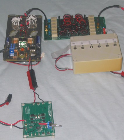
This picture above shows the amp connected to the LPF with a manual control box to set the LPF band (160–10M). In the final design, this manual control box does not exist. In the low cost version, a band switch will control it. The advanced model will automatically select the proper LPF according to the transceiver setting.
In my tests, the transistors will not be installed until I have the bias supply working correctly. That is really important in bringing up a new amp. The bias has to be right or you pop the transistors right away. I should get the few parts I need to complete the proto amp this week. My immediate goal is to get the bias working to my satisfaction, mount the RF transistors and start testing. I built this proto amp with the optional resistive pi network parts installed. I installed parts for -9dB.
After I am operational, I want to characterize the gain, current and band response from 160–10M. I find it useful to record the data into an Excel spreadsheet and plot it. It gives you a big picture. I have a keen interest to analyze the linearity to find the linear part of the operating curve. Low IMD is very high on my list of specifications to achieve. At some point soon I will have to get appropriate test equipment for IMD measurements.
In a word about packaging, I am planning on all flat panel designs for minimal costs. I have still not come up with a low-cost frame work, working on it in my minds eye right now.
Thank you for your support! I am sorry this could not be done faster. There are so many financial pressures to consider.
73, K5OOR – Virgil HF Projects
The AN758 Amp from CCI will be the benchmark for our amplifier. I received this amp kit from CCI last Friday. Natural convection cooling is out of the question unless you have a very large heat sink with a copper plate to move the heat from the heat source to the radiators. My goal is to enable 100% duty cycle operation. The HF SuperPacker Pro Version 2 used a copper heat sink with integral fan that worked well. The design for version 2 had the heat sink internal with the fan drawing air across the radiators and exiting the bottom of the box. There were several issues:
I picked this heat sink fan combination: http://www.micforg.co.jp/en/c_fs80e.html
The thermal resistance target for a single heat sink cooling two devices would be: 100-50/150 = .33 C/W
I ordered the model FS8025PU which has the heat sink with mounting hardware and a quality 80x25mm fan.

The heat sink/fan combination attaches to the rear of the circuit board with L-brackets. The fan passes through a cutout at the rear of the amp. Looking at the rear, you would see one inch of the fan body. The circuit board of the amp would be mounted on four 1 inch standoffs. Air flow design and fan noise will be a major consideration.
I am planning on a DC/DC Converter Module based on the Linear Technology LT3782EFE high power dual phase boost converter mounted stand-alone to provide up to 50V for the RF transistors.
I am starting to build the AN758 Module and hope to have it in test this week. We will do our own artwork incorporating additional circuits as needed.
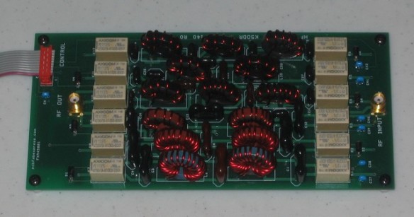
I have been getting some price quotes on dip silver mica caps used on the filter module. To get a decent price, we need to buy in volume. One manufacturer has a 1000 piece line item. I am shopping around for a reasonable supplier that will allow us to buy at least 100 sets of components at low cost.
73, K5OOR – Virgil
The WordPress.com stats helper monkeys prepared a 2012 annual report for this blog.

Here’s an excerpt:
600 people reached the top of Mt. Everest in 2012. This blog got about 8,000 views in 2012. If every person who reached the top of Mt. Everest viewed this blog, it would have taken 13 years to get that many views.
I have been having massive problems with the RF design I have using the RD100HHF1 MOSFET. I thought it would be easily accomplished like using the IRF510 but I have had troubles with the RF Input since day one. So much so that I am contemplating a change in direction.
On the HF SuperPacker1 and HF SuperPacker2, I used a design based on the Communication Concept Inc (Communication-concepts.com) AN762 (140W version). From this basic circuit board, I created our version which included all the support circuits, etc. See: http://site.hfprojectsyahoo.com/hf_superpacker_pro_ver_2 for details.
Now I more convinced I need to follow my past foot steps of development and start with the CCI AN758 Amplifier as the basis for this new amp. The AN758 is not a production design but is an engineering starting point as with other CCI products.
Hello,
While testing the new amp design, I recognized that the Input SWR from 160–10M was not staying low due to the coupling of my binary pr-resistive network to the amplifier input. I want to utilize the binary pi-resistive network so that the amp and various drive sources may be matched up. The binary pi-resistive network provides 1–15 dB in 1dB steps. It is controlled by a dip switch on the board. My problem was with 1dB attenuation the input SWR was not constant from 160–10M. I tried a lot of different solutions and finally came up with what I think is a good one. The current amp schematic in pdf form is attached. File Attachment: MOSFET AMP MODULE HFSPP V3.pdf (28 KB)
The solution I came up with is to use a 1:1 current balun using a 202–61 binocular core with #24 enamel wire. You can see the wiring of the core. The wire loops through a hole 3 turns. It is configured as a 1:1 current balun.


I invite any discussion about my impedance matching solution for this MOSFET type amplifier. The way the circuitry is laid out, I can have a isolated balanced input or have a low side common ground. I don’t find much literature or discussion about this sort of thing. My worse case test was on 10M with 1dB pi-resistive network. I measured 1.2:1. Other than that it was pretty much 1:1.
IF I can put this part of the circuit to bed, I can move on with power testing. I just wanted you to know that I am making progress and happy with this advancement.
73, K5OOR – Virgil
Hello group,
The current circuit board amp wide-band performance is not correct. I have to investigate the cause and correct.
This test is with 1W drive from 160–10M. We are looking for a flat dB gain characteristic. Obviously, we are not getting it but I am not discouraged. It is a mystery to solve.

I suspect the answer to be found in one of these areas:
73, K5OOR – Virgil
I have been working with the schematic and selecting parts that will allow me to mount all the panel parts on the PCB to eliminate wiring. This is what the circuit board looks like before it is routed.
See A/W parts placement below:
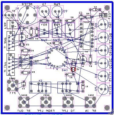
We have the row of SMA connectors at the bottom with the T/R relays just above that. The relays are placed on the panel side to give more finger room when attaching the SMA cables. The RF IN/OUT and PTT cables will run along the bottom of the case to the rear panel while LPF cables will route easiest path to the LPF module.
The two flat cables snap-in on the left side. One goes to the AMP and the other goes to the LPF. There is a row of LEDs mounted on the panel side that poke through corresponding holes on the front panel. The same goes for the three toggle switches and two LEDs at the top. A meter output jack allows you monitor the drain current for the MOSFETS. There is also a jack for a fan.
See the front panel drawing below:

This is what the front panel would look like. Note the size of the front panel. It is 1/2 inch wider and 1 1/2 inch taller than the HF PackerAmp V4. The hidden line is the circuit board dimension of 3×3 inch. Parts selection was important so that the toggle switches, rotary switch and LEDs have the same height.
You will be able to switch from CW to SSB optimization and turn the AMP on/off from the front panel. LEDs indicate TX and power. Your simple volt meter will allow you to set the bias and monitor amperage during transmit.
If you have comments or ideas, please feel free to share them with me.
73, K5OOR – Virgil
