Temperature Measurement Design Considerations Continued.

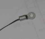
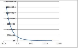
I have to linger on this subject because it is important in how this is done. I have the curves from the manufacturer of this 47K Thermistor. As you can see, it is very non linear.

Thermistor 47KThermistor 47K with 32.4K resistor

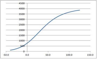
By adding a resistor we can manage the temperature measurement much better. Note that we now have a fairly linear curve from 0 to 127C.

In the attached Excel work sheet I calculate the current through the voltage divider using 5V as the reference. From the total current, we can calculate the voltage across the 32.4K resistor input to the ADC. Since we have a 12–bit ADC, we have 4096 counts range from 0 to 5V input. We now can create a two column 128 point lookup table in memory that correlates degrees C (0–127) in one column to ADC counts in the other.

One degree C resolution and relative accuracy is all we need to perform the MOSFET case temperature monitoring job. We could compute the temperature by solving a complex simultaneous equation but I elect to do it a fast and easy method of “binary divide and conquer”. It is possible to get the proper temperature by seven tests. The first test pointer is at the half way point in the lookup table of 64 degrees. “Is the lookup value higher or lower than the ADC count?” If higher, add 32 to the pointer. If lower subtract 32 from the pointer. Each test will reduce the power of 2 used to move the test pointer. Within 7 tests the pointer will be at the temperature reading. This algorithm can be done lightning fast in a iterative loop. The Excel spread sheet is attached:

File Attachment: Temperature Lookup table.xlsx (38 KB)

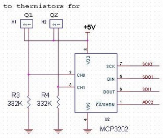
I created a drawing for my test fixture that shows me where to attach the wires on the Starter Kit I/O Expansion Board. We are going to use the SPI channel 1. The drawing shows 332K resistors but I settled on 32.4K as the optimum value.

File Attachment: STARTER KIT IO EXPANSION TEST.pdf (20 KB)

The little fixture (MCP3202 breadboard) will attach to J10. I hope to get that built tomorrow evening and wired, ready for writing a driver task. I have a logic analyzer and will post waveforms of the data acquisition. The software routine will be instructive on what goes on in a task. We will explore and hopefully enlighten those interested.


For more information: www.hfprojects.com

Signup for the HF SuperPacker Pro V3 by sending an email with your call sign and shipping address. No obligation for this interest list: vstamps@comcast.net

73 K5OOR –  Virgil HF Projects


Dual 12-bit ADC to read MOSFET temperatures

This week I am itching to start some program development using the PIC32 processor. We already have the freeRTOS ported to the processor. We established 3 empty independent tasks. I plan to add code to one of the tasks to control a Microchip MCP3202 CI/P chips. It is a dual channel 12–bit analog to digital converter.

MCP3202 ADC schematic crop

Notice the control lines on the right:

SCK1 is serial clock, SDO1 is serial data output, SDI1 is serial data input. These lines are all associated with SPI interface 1 of 2. SPI (serial peripheral interface) may be connected to many SPI devices and all share these 3 lines. Each part has a chip select. This signal is ADC2. When asserted low, the processor is talking to this part.

Link through Mouser Electronics to pdf data sheet For the breadboard, I am using the dip part. Click on the data sheet to view the details.

I selected a thermistor that can be used to monitor the temperature of each MOSFET.

Thermistors 003 crop

Each thermistor is placed under a screw head that mounts a MOSFET to the thermal block. The manufacturer provides a table of resistance values for the selected thermistor. It has been years since I created an interpolation table but it is no big deal. See the attached spread sheet. I notice VISHAY has one column that is a ratio of the thermistor resistance/ thermistor resistance at 25 degrees C. The column is per degree C from -40 to 125C. We are really not after absolute accuracy but a responsive reading of the thermistor. The processor task is to read the A/D values on a regular value, convert to degrees C and put the data in the data base.

Link through Mouser to 47K 3% thermistor data

File Attachment: RT_curve_NTCALUG03A473HC.xls (308 KB)

To get my feet wet with the new programming effort, I am constructing a bread board for the A/D chip and sensor. A flat cable will wire the signals over to the processor.

I will resume the BLOG after I get the connections figured out and the breadboard constructed.

73 K5OOR –  Virgil

HF Projects

Join the project. Send me an email: vstamps@comcast.net


Amplifier Design Refinements

When I develop a project I like to complete a portion and then savor the moment by doing other related tasks. Yesterday was such a day when I revisited the packaging requirements for the amp. I decided to change the amplifier length to make it symmetrical. Although only a 1.25 inch increase, there is now a balance. It also gave me the room to add a binary step pi-network adaptor on the input of the amp. This adaptor will allow the controller to adjust the RF input to match the drive conditions (0–15dB is 1dB steps).

The amp module will monitored for RF Input, temperature of each device, current, automated bias current adjustment. The amp is SPI controlled through a 16–pin flat cable and would possibly be great in a SDR spinoff application. See the attached schematic.

HFSPPROV3AMPPROTOAWHFSPPROV3AMPPROTOAWbottomHFSPPROV3AMPPROTOAWgroundHFSPPROV3AMPPROTOAWinner

From left to right: top, bottom, ground plane, inner routing layer

The layout is from bottom to top with an unbroken ground plane and three routing layers. The surface mount components are all located on the bottom.

The next step is further review and when I am able, to purchase a prototype circuit board and have fabricated a thermal block for heat transfer.

Thanks for your support and I look forward to adding your call to our list of builders. send an email to vstamps@comcast.net . You will be contacted when we are ready to begin the build.

73 K5OOR –  Virgil

HF Projects


File Attachment: HF SuperPacker Pro 100W Amp V3 Schematic.pdf (27 KB)


HF SuperPacker Pro 100W Amp Module Layout Detail 9/6/2011


I appreciate it very much that you have taken the time to stop by and learn more about the new amp design.

You are seeing the internal detail showing how the circuit board, thermal block, heat sink and skin are connected to each other. The heat sink is attached to the skin. The thermal block is attached to the heat sink through a skin cutout. The circuit board is attached to the thermal block. The MOSFETs are attached to the thermal block with circuit board cut outs in the circuit board to allow the MOSFETs to be mounted to the thermal block. The tabs of the MOSFETs solder to the top side of the circuit board.

The thermal block drawing was modified to add built in spacing to hold the MOSFETs at the proper distance. The thermal block mounts flush with the bottom of the circuit board. The surfaces are milled flat with spacing needed for MOSFET flush mounting. You can zoom the attached file for more detail.

I decided to add 1.25 inch to the left side of the circuit board to make the whole assembly symmetrical. I am going to add to the artwork for the binary tree pi network circuits for input range adjustment. 

I envision the amp to have a height of 3.5 inch which will be sufficient room for the optional touch screen display on the front. Along the back and sides will be heat sinks for the optional RF modules.

There is a lot to think about and consider. I want to get this major module into prototype hardware as soon as funds will allow. I would appreciate your financial help in the R&D process: R&D Support

Sign up for the project. Send email to vstamps@comcast.net with your call sign and shipping address. No obligation until call for payment.

Amp module layout hfspprov3

File Attachment: amp mounting detail hfspprov3.pdf (14 KB)

HF SuperPacker Pro Ver 3 Amplifier Developments

Hello all. This is my first communication using a BLOG to tell you about developments of the latest project from hfprojects . The HF SuperPacker Pro 100W Amplifier is in its 3rd version since 2006. Each version builds upon past designs and moves forward with what is possible now. We exist to create home construction projects for the Radio Amateur. The designs are from Virgil – K5OOR who creates the projects, writes the construction manuals, stages the parts and delivers the projects to the builder. We have been at it since 2000 with thousands of home construction projects shipped world-wide.

I have posted several prior reports using pdf. You can review them here to follow along and catch up to the current state of developments.

Specifications and Goals

Progress Report 8/14/11

Progress Report 8/19/11

Progress Report 8/26/11

Progress Report 9/3/11

Now lets fast forward to today. I have not figured out how to work this BLOG to do what I want to do so please be patient.

HF SUPER PACKER PRO V3 AMPLIFIER MODULE Part 3


This is the artwork for the Rev 0 (prototype) HF SuperPacker Pro V3 100W Amplifier Module. This design uses two MOSFET transistors operating with 48V drain voltage. The board is a four-layer design with the blue traces on the bottom layer and red traces on the top layer. In the middle is an unbroken ground layer. There is one additional internal routing layer. The interface is SPI which controls the bias, measures the current and the temperature of each MOSFET. A 10-pin flat cable connects the amp controls to the planned PIC32 Processor.

3/8” thk tapped Aluminum Block.

The MOSFET transistors mount to a thermal transfer block (shown above).  The thermal transfer block attaches to a case heat sink. RF In/Out utilizes SMA connectors.  (3 inch by 5 inch circuit board)

The RF Input is contemplated to be driven from a binary tree pi network ranging from 1 – 16 dB of variable attenuation. It is not known how well this is going to perform with a 48V drain but if my experience holds true, there will be additional gain and make the requirement for a SDR preamp go away. The RF drive portion of the design will be confirmed after evaluation of this prototype. Sign up for this version 3 HF SuperPacker Pro 100W Amp, send to vstamps@comcast.net your call sign and shipping address. No obligation.

I want to go forward by having a minimum order of this prototype board fabricated and one of the heat transfer blocks fabricated. I estimate $200 is needed to create these two prototype items. With them, I can confirm this major part of the design and write the software driver to control it. We can’t do it without your support. R&D Development is an expensive process with all the prototyping and design efforts. You can participate: purchase HF SuperPacker Pro 100W Amp V3 R&D Support at the store: http://www.hfprojectsyahoo.com/hfsupro10amp.html . Your support is vital and very much appreciated. Thanks all who participate with me. Our speed of development is controlled in large part by funds available for the R&D effort.

On the software front, we have integrated the trace function into our REAL ICE emulator. This is a major tool used in software development.

73, K5OOR – Virgil